About the project
My studies in nanotechnology with the focus on nanoelectronics had several interesting course projects. The project was carried out at the MST (Division of Micro and Nanosystems) at the
School of Electrical Engineering and Computer Science (EECS) at KTH Royal Institute of Technology in Stockholm, Sweden. For the course EK2360 Hands-on MEMS Engineering,
students carried out a project in the field of Microsystems engineering. The purpose of the project was to design, fabricate and evaluate a system for an optical switch. The system
needed to be fabricated in silicon, should be movable in two directions and should have the possibility to be locked in to place at specific distances from the origin.
Fun fact!
Mechanical multi-stable optical in-plane switch design
Project description
For the course EK2360 Hands-on MEMS Engineering, students were tasked with
designing, fabricating, and evaluating a system for an optical switch. The requirements were that
the system should be fabricated in silicon, be movable in two directions, and have the capability
to be locked in place at specific distances from the origin. The design goal was to create a switch
that could move ±15 μm in either direction and be precisely controlled as well as locked within this range.
The system should also be possible to control linearly, by adjusting the applied voltage to the electrodes.
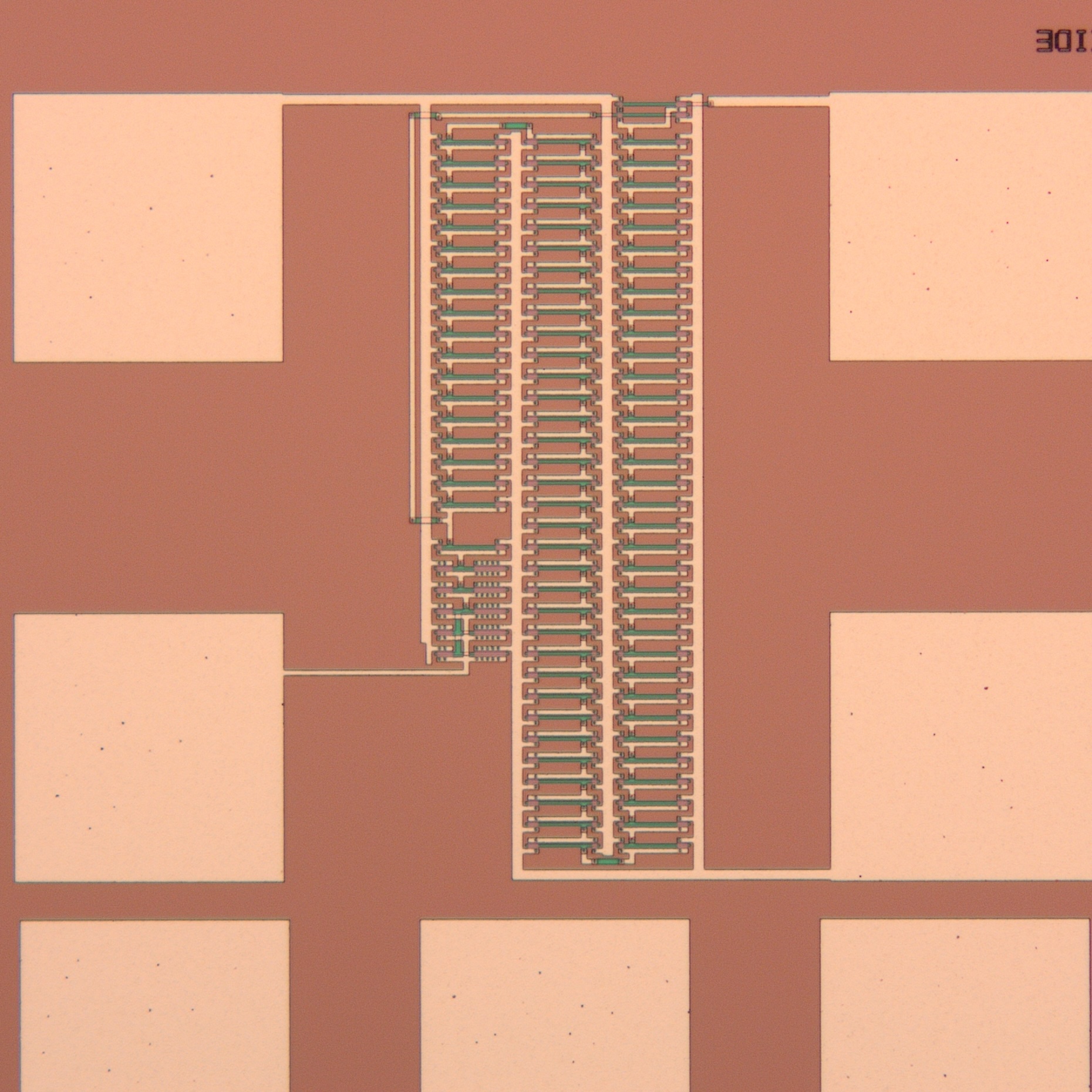
The MEMS system design focused on an electrostatic actuation mechanism using a comb drive system. This choice allowed for large displacement (±15 µm) and a stable control region. The spring system consisted of folded springs with anchor points, providing flexibility in adjusting properties. The spring constant k was a crucial parameter, responsible for defining the spring's properties in the desired direction as well as in unwanted directions to prevent lateral instability or transverse motion. Two basic designs were simulated using COMSOL for FEM-analysis, iteratively refining the designs. Important properties such as lateral and rotational stability, stable range of the actuator, and spring constants were simulated and adjusted accordingly. Final designs were implemented in AutoCAD for chip layout, accommodating about 50 individual devices, including devices from the mandatory designs as well as the alternative device designs.
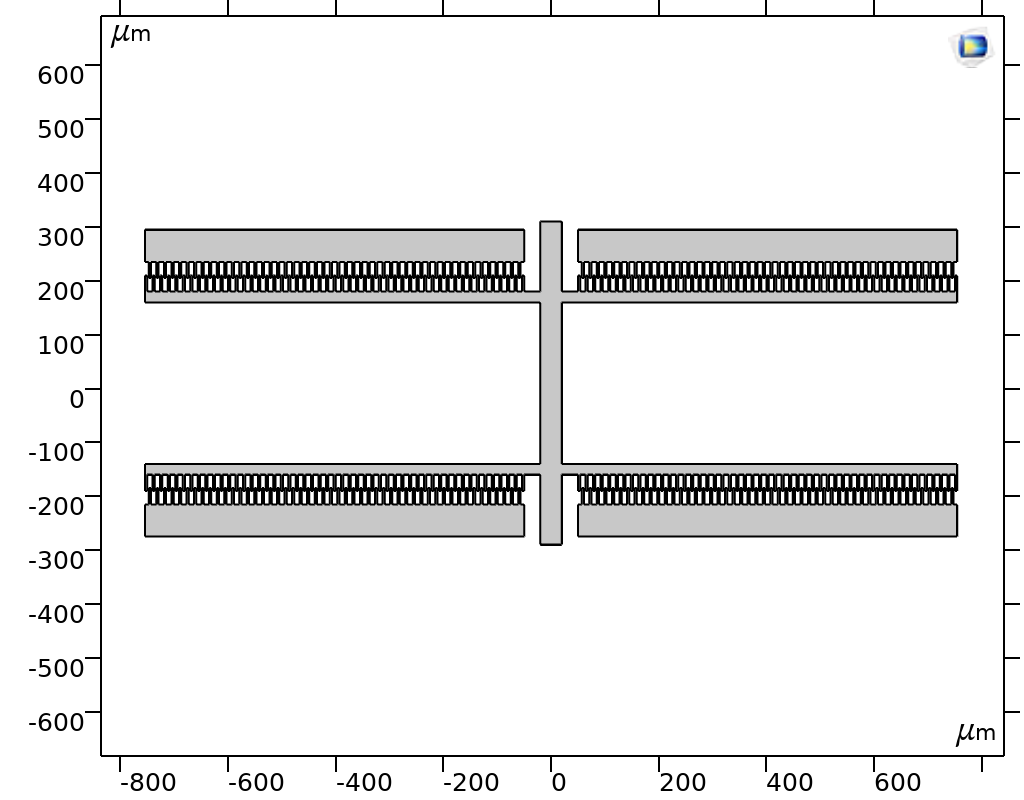
Springs used to move the device when applying a potential
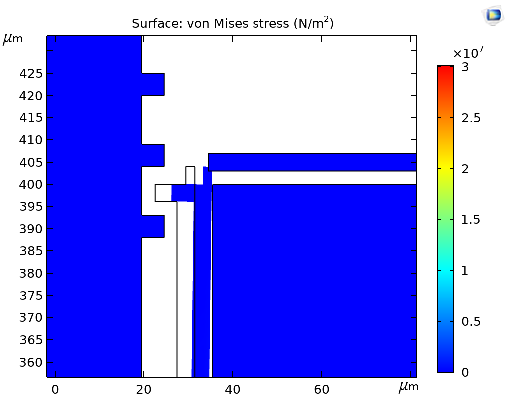
Locking mechanism of the device simulated using COMSOL
Fabrication
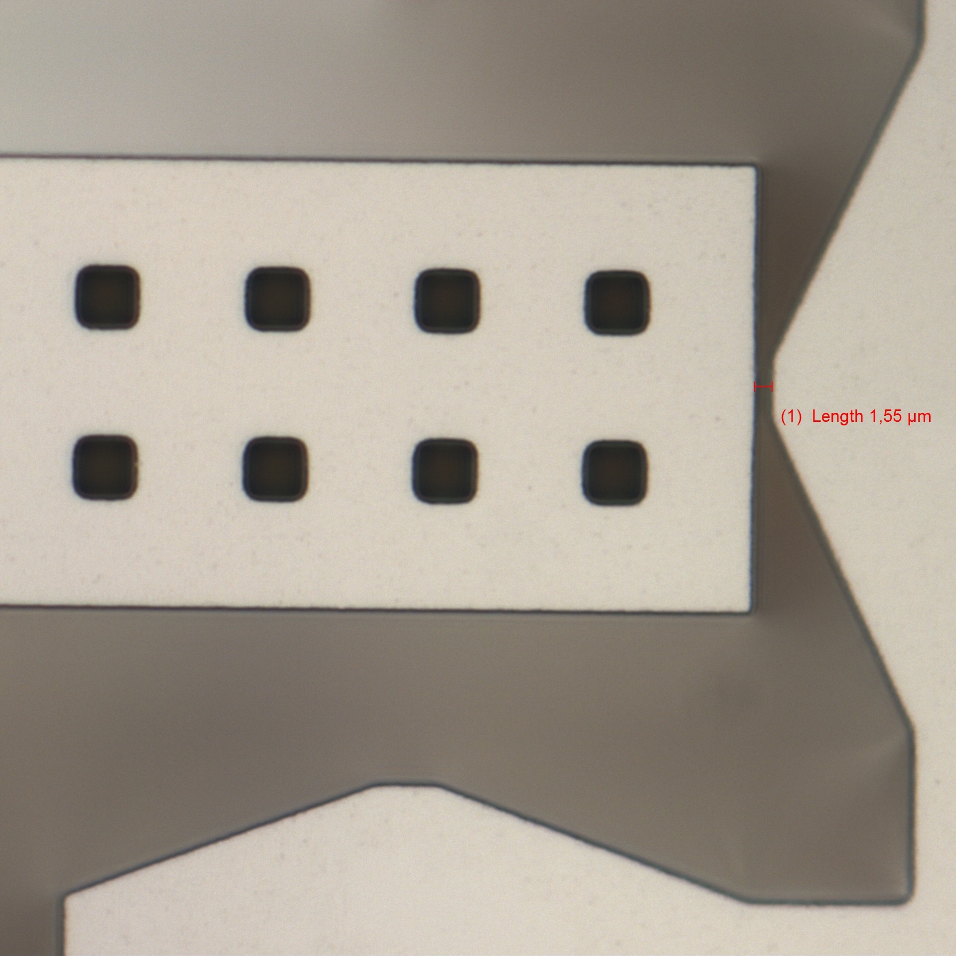
Fabrication began with a Silicon on Insulator (SOI) wafer, involving photoresist coating, mask alignment, and UV patterning. Deep Reactive Ion Etching (DRIE) using the Bosch process created precise structures. This process allowed for high aspect ratio etching, achieving 47μm deep trenches with only 3.31μm diameter. Subsequent steps included wafer dicing, structure release using HF acid etch, critical point drying to avoid stiction, and aluminum metallization for electrical contacts. The HF etch lasted about three minutes at an etch rate of 1.5nm/min. Critical Point Drying (CPD) was used to avoid surface tension forces and stiction of moving parts during the drying process. Post-fabrication inspection used Light Optical Microscopy (LOM) and Scanning Electron Microscopy (SEM), revealing successful releases and some stuck structures. SEM imaging allowed for observation of different parts of the device, including the locking mechanism, comb fingers, and spring system. Measurements showed fabricated geometries were within ±1 µm of the design, with a tendency for smaller features in areas with more etched space around them.
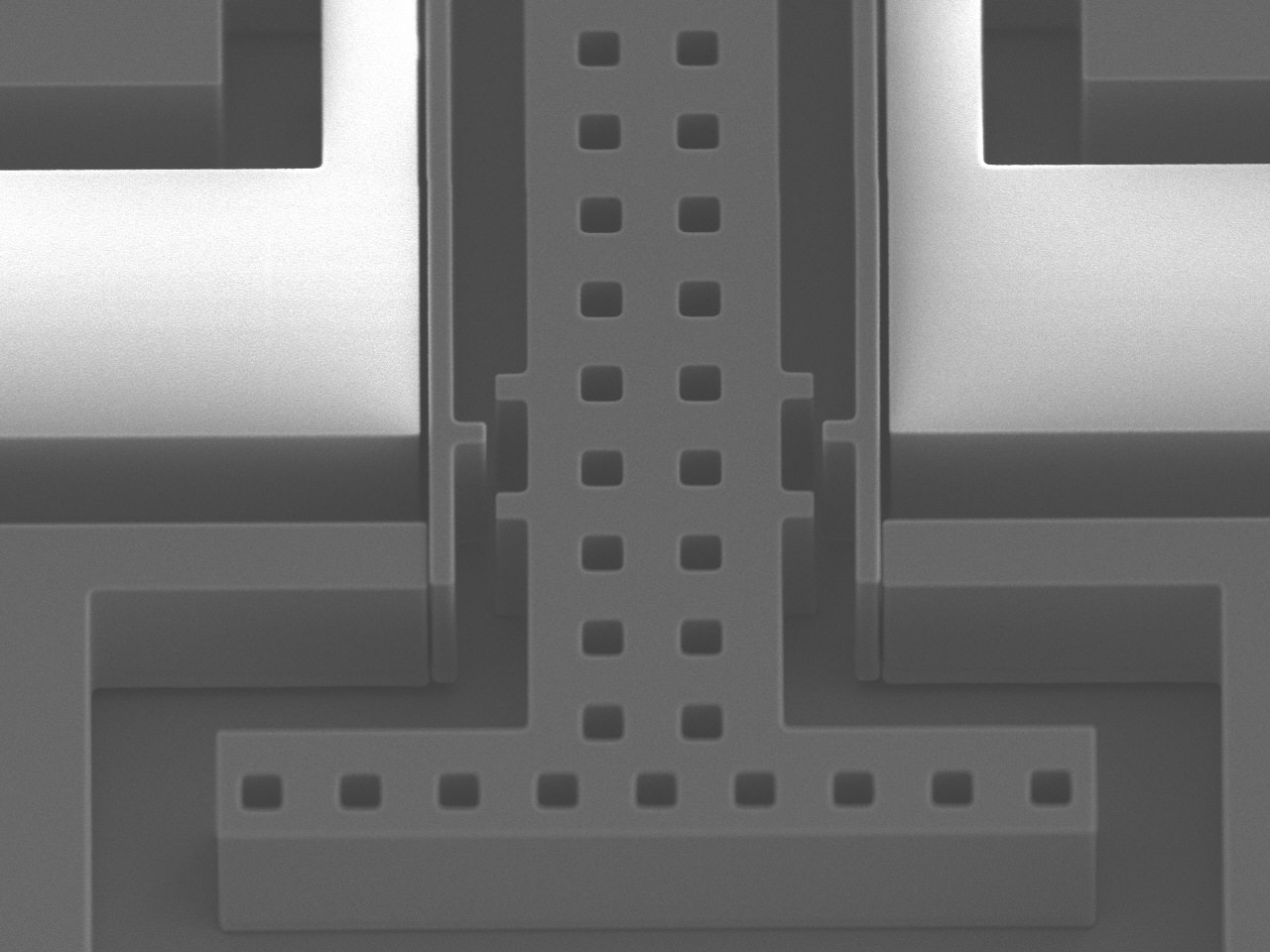
Locking mechanism used to hold the springs in place
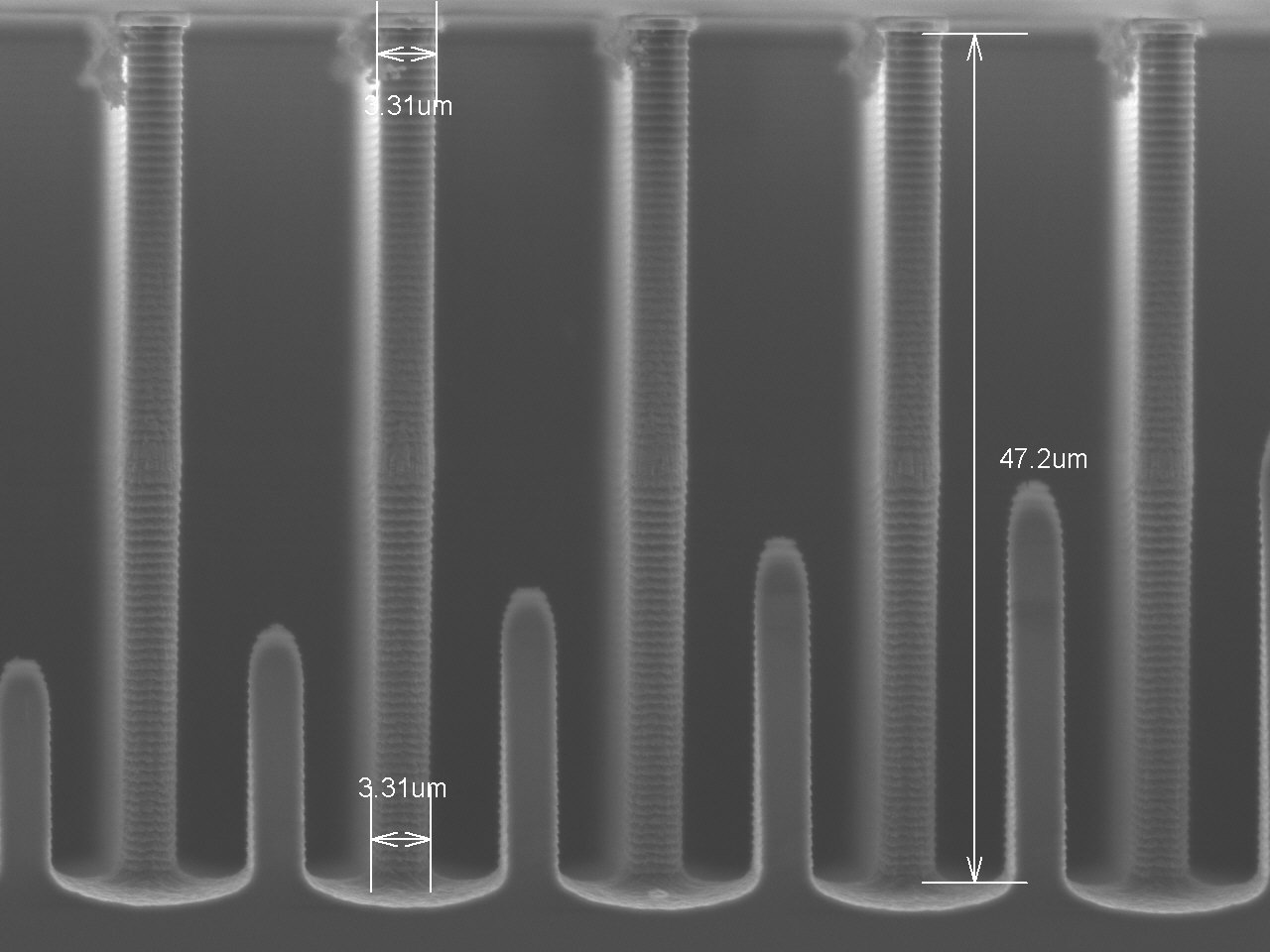
Deep trenches etched into the silicon
Results
Testing revealed varying yields across different designs. The main design showed 15% fully functional devices when testing only actuation, increasing to 25% when testing both actuation and locking mechanism. Secondary designs performed poorly, likely due to inferior rotational stability. Common issues included stuck movable parts and partially functional locking mechanisms. Real-world devices required lower voltages than simulated (28.5V vs 65V) to operate the locking mechanism, possibly due to under-etching or unaccounted pull-in effects. This discrepancy might be attributed to the locking mechanism behaving similarly to a parallel plate actuator, where pull-in occurs after moving 1/3 of the initial gap. Secondary designs (B and D) showed less stability, rotating at voltages above 50V, unlike the main design. This instability was expected based on the simulation results. While some design parameters like rotational and lateral stability couldn't be directly measured during characterization, the observed behavior of the secondary designs aligned with the predicted lower rigidity and stability.
Contributions to the project:
- Designed and simulated two versions of the optical switch using COMSOL Multiphysics
- Optimized the comb drive actuator and spring system for precise control and stability
- Participated in the fabrication process, including photolithography and DRIE
- Conducted post-fabrication analysis using LOM and SEM imaging
- Performed device testing and characterization, analyzing the performance of different designs
- Contributed to the final project report, documenting the design process, fabrication steps, and results
What I learned from this project:
This project provided me with invaluable hands-on experience in MEMS design, fabrication, and characterization.
I gained deep insights into the challenges of creating microscale electromechanical systems, particularly
focusing on optical switches. My understanding of microfabrication techniques expanded significantly,
especially in areas such as photolithography, deep reactive ion etching, and critical point drying.
I learned to use advanced simulation tools like COMSOL Multiphysics to optimize designs before fabrication,
which proved crucial in predicting device behavior and improving performance. The project also enhanced my
skills in clean room protocols and microscopy techniques, including SEM imaging and analysis.
Furthermore, this experience taught me the importance of iterative design and the challenges of translating
theoretical designs into practical devices. I gained a deeper appreciation for the complexities involved in
MEMS fabrication, including the impact of small variations in the manufacturing process on device performance.
Overall, this project significantly improved my problem-solving skills in a research and development context,
teaching me to adapt and learn quickly when faced with unexpected results or fabrication challenges.
