About the project
My studies in nanotechnology with a focus on nanoelectronics included several fascinating course projects. This particular project was conducted at the
School of Electrical Engineering and Computer Science (EECS) at KTH Royal Institute of Technology in Stockholm, Sweden.
As part of the course on semiconductor device fabrication, students participated in a hands-on project in the field of MOSFET manufacturing.
The purpose of the project was to complete the final step in a MOSFET preparation process on a CMOS wafer by adding metal contacts to enable
communication between CMOS transistors. The project required working in a cleanroom environment and involved various microfabrication techniques
including photolithography, metal deposition, and reactive ion etching. The project was supervised by Per-Erik Hellström, providing invaluable guidance
throughout the process.
Read the project report here
Fun fact!
MOSFET Interconnect Deposition and Reactive Ion Etching
Project description
This project focused on the final step of a MOSFET preparation process on a CMOS wafer developed
by the Department of Electronics at KTH Royal Institute of Technology. The main objective was to
add metal contacts that enable communication between CMOS transistors. The project aimed to provide
hands-on experience in a cleanroom environment and involve depositing metal on transistor contact
holes prepared by another lab group.
The experimental work involved several key steps. First, SiO2 etching was performed to remove a thin layer of oxide (20-30 nm) inside the contact holes using a 1% HF solution. The wafer was placed on a spinning platform and etched for 45 seconds, then rinsed with water to stop the process. Next, metal deposition was carried out using the Endura PVD system to deposit a layer of 100 nm TiW/500 nm Al. This system uses sputtering deposition, where argon gas is accelerated towards a cathode target, and the sputtered atoms coat the substrate with a thin film. The photolithography step involved coating the wafer with photoresist, soft-baking, and then exposing it using a Nikon NSR Stepper. This step defined the pattern for the metal contacts. Metal etching was performed using Reactive Ion Etching (RIE) to remove unwanted parts of the metal layer. This dry etching technique uses a chemically reactive plasma to etch the exposed aluminum with high selectivity and anisotropy. Finally, resist stripping was carried out to remove the remaining photoresist using dry stripping with plasma etching equipment at an elevated temperature.
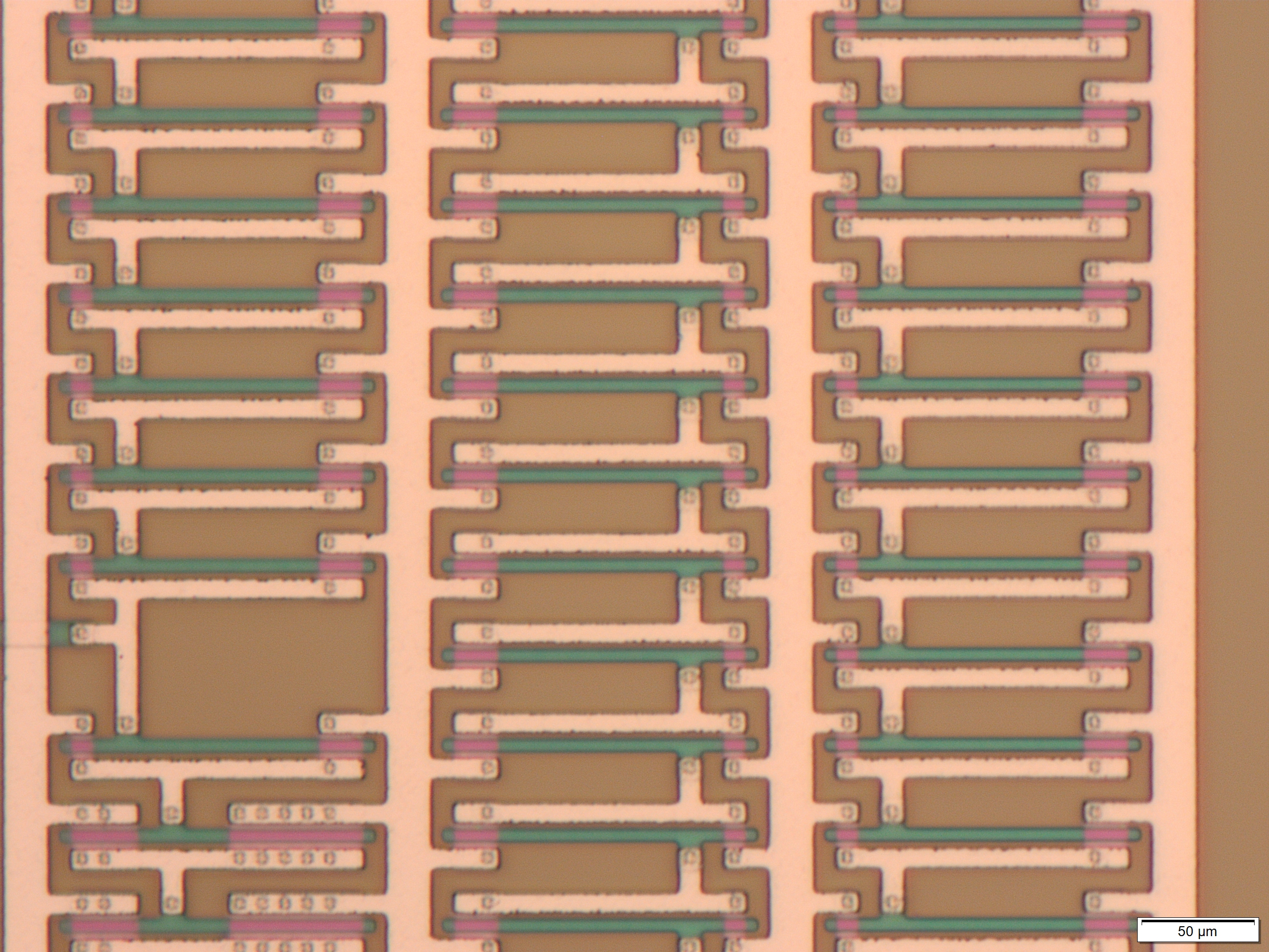
The individual transistors after resist strip
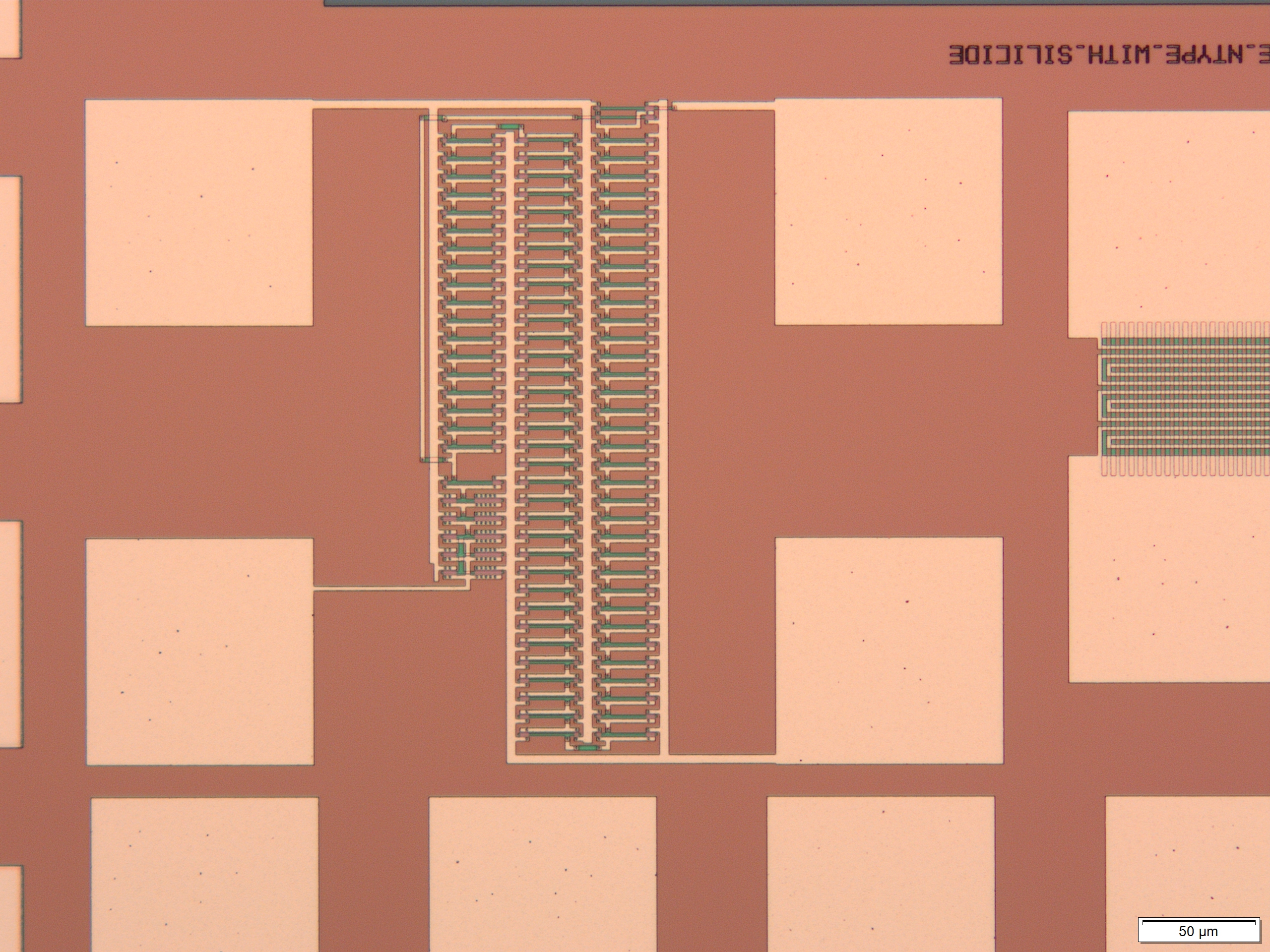
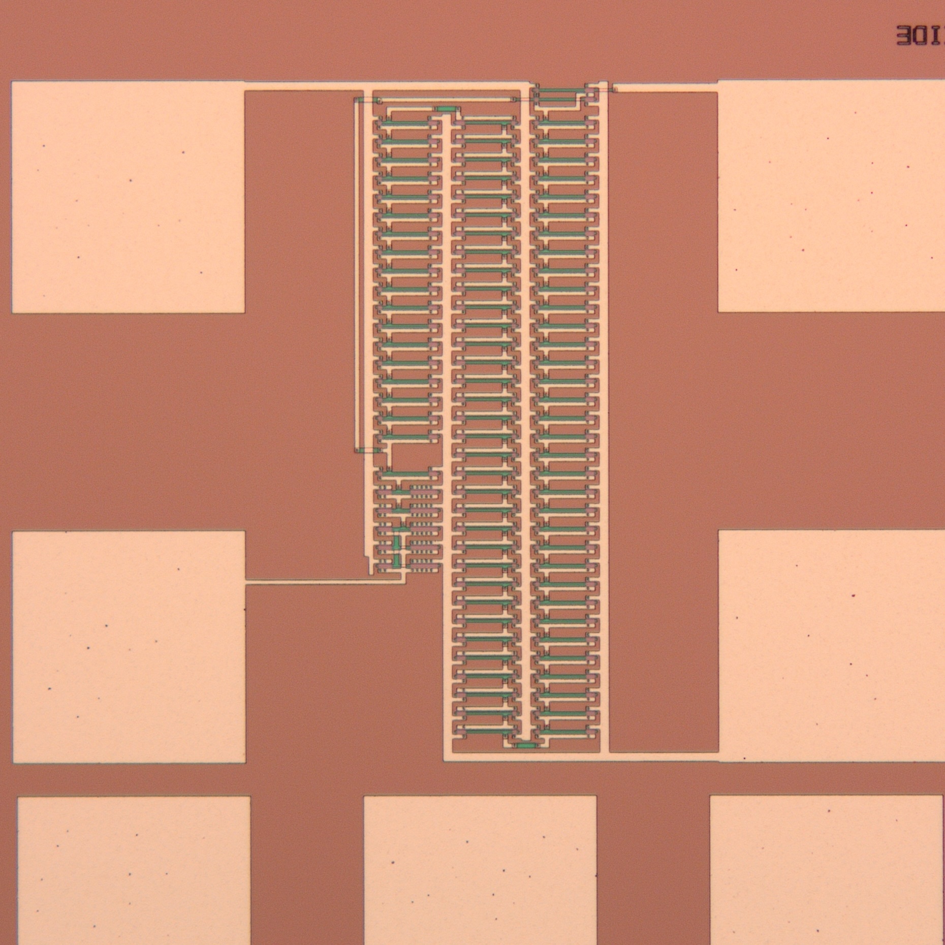
Network of MOSFETs forming an integrated circuit
Results
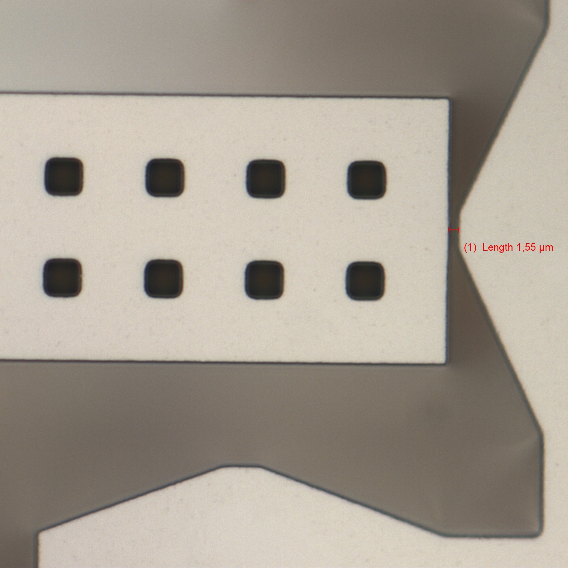
The project yielded several significant results. The metal layer thickness was calculated to be 450 nm using sheet resistance measurements, close to the target of 500 nm for the Al layer. The fabrication process achieved a resolution of approximately 0.8 μm, sufficient for creating the 1 μm contact holes without risking short-circuits. Both the wet etch and RIE processes demonstrated good anisotropy, producing metal lines close to the target thickness of 1 μm. Notably, the alignment accuracy of the photolithography process was particularly impressive, showcasing the precision of the Nikon NSR Stepper.
Contributions to the project
- Performed SiO2 etching to prepare contact holes for metal deposition
- Operated the Endura PVD system for metal layer deposition
- Conducted photolithography processes, including resist application and development
- Carried out RIE for precise metal etching
- Analyzed results using sheet resistance measurements and microscopy techniques
What I learned from this project
This project provided invaluable hands-on experience in semiconductor fabrication processes. I gained practical understanding of cleanroom protocols and the importance of precision in nanofabrication. Working with advanced equipment like the Endura PVD system and Nikon NSR Stepper deepened my comprehension of various etching techniques and their impact on device structures. I developed a greater appreciation for the complexity of CMOS fabrication and the interplay between different process steps. The project also honed my skills in analyzing and interpreting results from semiconductor fabrication processes. Perhaps most importantly, I learned the critical importance of attention to detail and patience in achieving high-quality results in nanofabrication. Overall, this project bridged the gap between theoretical knowledge and practical application in semiconductor device fabrication, providing a solid foundation for future work in this field.
